With the growth of IT industry, a large variety of new materials just like the bamboo shoot in spring come out overnight after a sweet rain. Now the semiconductor material has rapidly developed and become the foundation of IT industry that could never subsist without the support of semiconductor material which is acted as a bridge over the two sides of human being and the information super highway and also is a bond linking us with the modern life. As one of major semiconductor materials, silicon wafer has been widely used in the field of telecommunication, science research, manufacture and common life, etc. In recent years, the demand in the international market for the silicon wafer has been dramatically swelled, so the manufacturer has rack their brain to speed up the technological innovation and schemed to expand the production scale so that the silicon wafer they produced have gone through a continual improvement of quality. In order to meet the requirement of developing of IT industry and meanwhile maintain a increasing share of the market under the tense competition, now, the manufacturers are forwarding to increase the diameter of the wafer and also try to minimize the harmful particles and defects on the wafer to assure their customers of a high-quality product.
Asia is the major base of manufacturing of semiconductor materials in the world and has the most advanced related techniques and product line. Sino surplus as a member in this field is able to provide you with the semiconductor materials of high-level quality and also can assure you of a reliable and prompt service to your full satisfaction.
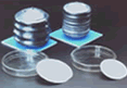
Silicon is the material that the majority of the semiconductors and microchips are built on. Ironically, silicon by itself doesn't conduct electricity very well. However it can take on the dopants precisely in order to control the resistivity to an exact specification. The most common dopants are boron, phosphorus, arsenic, and antimony. Depending on which dopant is used, silicon wafer are classified into a P or N type (Boron: P type; phosphorus, Arsenic, Antimony: N type). When the monocystaline silicon ingot is made through the method of CZ or FZ and then go through a consecutive process of slicing, edge grinding, lapping, etching, polishing, and cleaning, the finished silicon wafer is firmed and accordingly called slice wafer, etch wafer, polish wafer, or Fz wafer, etc. now Sino surplus can supply all kinds of silicon wafer and GaAs wafer for all diameters ranging from ? 1.5 ? - ? 12 ? in accordance with the customers' requirement.
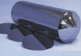
Monocrystalline silicon ingot
Type/Dopant : P/Boron; N/phosphorus
Orientation : {100} /{111}/ {110}
Diameter : 1.5" - 12"
Resistivity : 10 - 3 - 80O.cm
Radial resistivity variation: No
Minority carrier Lifetime: = 10 ?s
Defect: None
Note: other specification depends on the customers' requirement
Cutting and grinded wafer
Diameter :
F 1.5 " -
F 12 "
TTV: <5 ?m
GTIR: < 3 ?m
Bow/Warp: <20 ?m
Note: other specification depends on the customers' requirement
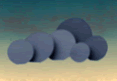
200mm polish silicon wafer
Growth Method : Cz
Diameter : 200 ± 0.2 mm
Type/Dopant : P/Boron; N/phosphorus
Orientation : {100} /{111}
Resistivity : 0.003-50ohm.cm
Radial resistivity variation: P type < 5%
N type < 15%
Metals : < 5xE10
Metal of surface: Copper, Chromium, Iron, Nickel = 2.5 xE10
Aluminum, zinc, Calcium, Sodium = 1.0 xE11
Oxygen concentration: (5.0-7.8) x E17 ± 0.5
Radial Oxygen variation: 5%MAX
Carbon concentration: = 2.0 x E17
Thickness : follow SEMI standard or customers' requirement
TTV : < 3 ?m
GTIR: < 2.0 ?m
Site Flatness (STIR) : < 0.3 ?m
Bow/Warp : < 20 ?m
Particle Count : <30@>0.15 ?m
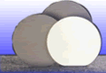
150mm silicon wafer
Growth method: CZ
Diameter(tolerance): 150.0 ± 0.2mm
Thickness: follow SEMI standard or customers' requirement
Type/dopant: P/Boron ; N/phosphorus
Orientation: <100>/<111>
Resistivity: 0.003-50ohm.cm
Radial resisitivity variation: P type < 6%
N type < 25%
Oxygen concentration: 5.0-7.8 x E17 ± 0.5
Radial Oxygen variation: < 5%
Carbon concentration: = 2.0 x E16
Metals: = 1.0 xE11
Metal of surface: Copper, Chromium, Iron, Nickel = 5 xE10
Aluminum, Zinc, Sodium, Calcium = 2.0 xE11
TTV: < 2.5 ?m
GTIR: <1.2 ?m
STIR: < 0.3 ?m
Bow/Warp: < 30 ?m
Particle Count : <30@>0.2 ?m
Note: above parameters depend on the customers' requirement
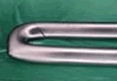
Polycrystalline silicon rod
The diameter: 40-200mm
Diameter tolerance: = 10%
Donor: > 3000
O . ?
Acceptor: > 300
O . ?
Carbon content: 2xE16at/?3
Note: above parameters depend on the customers' requirement.
Silicon powder
Purity:99.999%
Particle size: not above 600 mesh.
Note: other specification is available upon
request.
Semi-insulating GaAs wafer
Diameter: 2 ? ?6 ?
Dopant: non-dopant / Cr
Orientation: <100>/<111>
Maching: sliced or polished wafer are available on request
Low-resistivity GaAs wafer
Diameter: 2 ? or 3 ?
Dopant: Si/Cr
Orient: <100>/<111>
Machining: sliced and polished wafers are available on request.
Note: other specification is available upon request.
|